


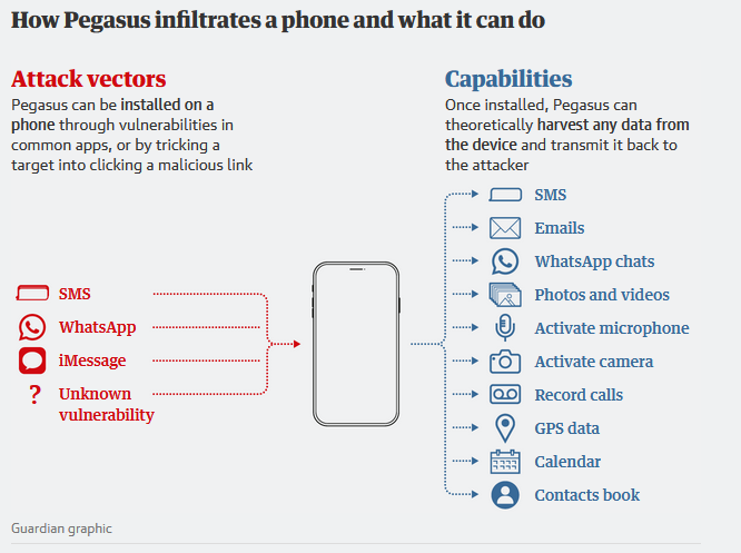
.png)
 - Vertical.png)
.png)
 - Vertical.png)
.svg)
.png)
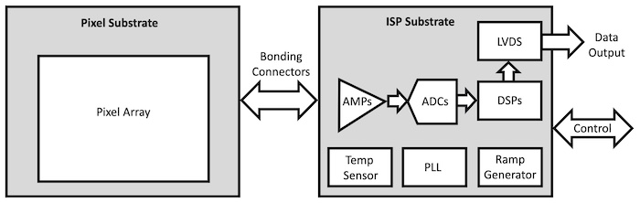
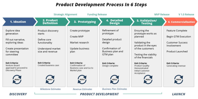
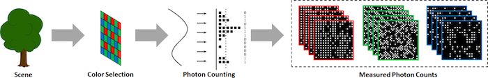
Very Large Scale Integration
Difficulties
- Process variation - As photolithography techniques get close to the fundamental laws of optics, achieving high accuracy in doping concentrations and etched wires are becoming more difficult and prone to errors due to variation.
- Stricter design rules - Due to lithography and etch issues with scaling, Design Rule Checking for layout has become increasingly stringent. This means designers would have to keep in mind a large number of rules when laying out custom circuits. This is reaching a point where design houses are now opting to switch to Electronic Design Automation (EDA/ECAD).
- Timing/Design closure - As clock frequencies tend to scale up, desingers are finding it more difficult to maintain low Clock Skew between high frequency clocks across the chip. This has led to the development of multicore and multi-processor architectures, since an overall speedup can be obtained even with lower clock frequency by using the computational power of all the cores.
- FIrst-pass success - As die sizes shrink (due to scaling) and wafer sizes go up (due to lower costs), the number of dies per wafers go up, and it become more complex to make suitable photomasks. A mask set for a modern technology can cost millions of dollars. Because of this, we have to abandon the old philisophy of using several spin-cycles to find errors in silicon, and resort to first pass success. Several design philosophies have been developed to aid this new design flow, including Design For Manufacturing, Design For Test and Design For X.
- Electromigration